Semiconductor materials are one type of element which has a special class of conductivity between a good conductor and an insulator.
Semiconductor materials can be two classes: one is the single crystal semiconductor (Germanium, Silicon) which has a sequential bonding of one material. And Another is the compound semiconductor (Gallium Arsenide, Cadmium Sulphide, Gallium Nitride, Gallium Arsenide phosphide) which have a bonding structure of two or more materials. The most used semiconductor materials in solid-state electronic devices are Silicon, Germanium, and gallium arsenide.
Semiconductor materials are generally formed with covalent bonding. Covalent bonding is the bonding of atoms by the sharing of electrons.
Here are two types of semiconductor:
- Intrinsic: It has a very low level of impurities that tend to pure elements and has four valence electrons.
- Extrinsic: It contains predefined impurity (n-type or p-type) materials by the doping process.
n-type and p-type semiconductor materials
Doping process
The ability to change the characteristics of a material by adding impurity to a pure semiconductor material is known as doping.
Semiconductor materials are tetravalent. N-type material is formed by adding impurity elements that have five valance electrons (Phosphorous, Arsenic, Antimony). And a p-type material is formed by adding impurity elements that have three valance electrons (Boron, Gallium, Indium).
An n-type material contains a large number of electrons than holes because pentavalent material is added to the pure semiconductor material. For p-type material, it has more holes than electrons for the addition of trivalent material. Both p-type and n-type material is electrically neutral.
A table of majority and minority charge carrier for the p-type and n-type material:
| Charge carrier | n-type | p-type |
| Majority | electrons | holes |
| Minority | holes | Electrons |
Energy levels
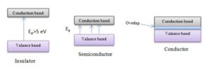
For the isolated atomic structure of every element, it has a valance band, conduction band, and an energy gap between them. Insulator has the highest energy gap (Eg>5eV), the semiconductor has a special energy gap in between insulator & conductor material, and the conductor overlaps its conduction band & valance band. There is no energy gap in the conductor element. The higher is the energy gap, the larger is the amount of absorbed energy and it is because of the free charge carrier. The energy gap is measured by the electric volts (1eV= 1.6*10-19J).
The electron of the valance band is not reachable to the conduction band for the insulator; in semiconductor, it is reachable to get conduction and electron flows when reached. For Silicon semiconductor Eg=1.1eV.
Temperature effect on semiconductor materials
The difference between semiconductor and conductor material is employed by applying heat on it. With the increase in heat, conductor material shows the resistivity increasing property, on the contrary, the semiconductor material exhibits its conductivity increasing.
Conductor and semiconductor materials have a positive and negative temperature coefficient respectively.
Analyze yourself:
| Q1. What is a semiconductor? |
| Q2. Discuss the doping process. |
| Q3. Discuss the temperature effect on the semiconductor material. |


